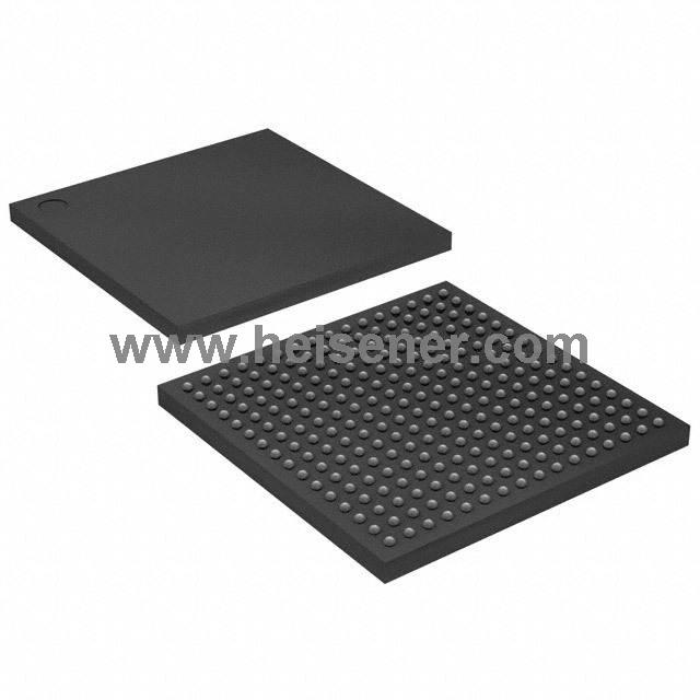
The EPCS4SI8N is a 4-Mbit serial configuration device housed in an 8-pin SOIC package. It is part of the EPCS flash family designed to store FPGA configuration data and automatically provide it upon power-up for device initialization. This device works seamlessly with all FPGA families and supports Active Serial (AS) x1 configuration schemes.
Beyond configuration, unused memory space in the EPCS4SI8N can be accessed through the Nios® processor and SOPC Builder system for data storage or retrieval using the flash memory system. Additionally, it supports in-system programming through the JTAG interface, enabling FPGA devices to program or update the flash contents without removing the component from the board.

nCS (Chip Select) – Active-low signal used to enable the device. When low, the EPCS4SI8N listens to commands and data on the SPI bus.
DATA (DO) – Serial data output pin. The stored configuration data or memory content is shifted out through this pin during read or configuration operations.
VCC – Power supply pin. Provides the necessary operating voltage for the device.
GND – Ground reference for the device.
ASDI (DI) – Serial data input pin. Used to input configuration data, instructions, or memory contents into the device.
DCLK (Serial Clock) – Provides the clock signal for synchronizing data transfer between the FPGA and the EPCS device.


| Parameter | Specification |
| Manufacturer | Altera |
| Memory Density | 4Mb |
| Package Type | 8-SOIC |
| Interface | SPI (Serial Peripheral Interface) |
| Configuration Mode | Active Serial (AS) x1 |
| Operating Voltage (Vcc) | 2.7V ~ 3.6V |
| Clock Frequency | 40 MHz |
| Data I/O Pins | ASDI (input), DATA (output) |
| Operating Temperature | -40°C ~ 85°C |
Easy-to-use four-pin interface
Low cost, low pin count and non-volatile memory
Low current during configuration and near-zero standby mode current
3.3-V operation
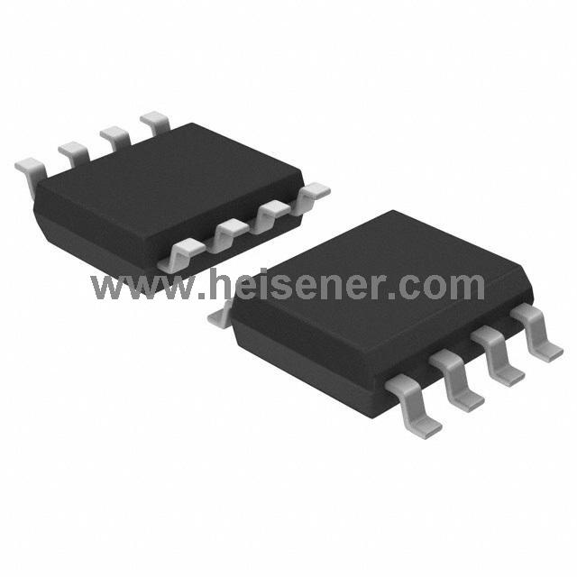
Available in 8-pin small outline integrated circuit (SOIC) package
Enables the Nios processor to access unused flash memory through active serial (AS) memory interface
Re-programmable memory with more than 100,000 erase/program cycles
Programming support with ByteBlasterTM II download cable
Additional programming support with Altera
Programming Unit (APU) and programming hardware from BP Microsystems, System General, and other vendors
Software design support with the Altera Quartus II development system for Windows-based PCs as well as Sun SPARC station and HP 9000 Series 700/800
FPGA Configuration Storage
Embedded Design and Development
In-System Programming
Industrial Control Systems
Communication Equipment
Consumer Electronics

This diagram shows the internal block structure of the EPCS4SI8N. When the nCS (chip select) signal is pulled low and the DCLK (clock) provides pulses, the control logic activates the data transfer process. External input data enters through ASDI (data input) into the I/O shift register. With the help of the address counter and decode logic, the data is accurately written into the internal memory array.
On the other hand, when data needs to be read, the contents of the memory array pass through the data buffer and are finally sent out via the DATA (data output) pin. At the same time, the status register keeps track of the device’s working state, such as whether it is busy with write or erase operations, allowing external devices to monitor progress. The entire process relies on SPI serial communication, which simplifies circuit connections while ensuring the FPGA can reliably and efficiently receive the configuration data it needs.
EPCS1SI8N: 1 Mbit of storage, suitable for small FPGA configuration needs.
EPCS4SI8N: 4 Mbit of storage, a common choice for medium-sized FPGAs.
EPCS8SI8N: 8 Mbit of storage, ideal for configuration projects with larger data volumes.
EPCS16SI8N: 16 Mbit of storage, supports complex and large-scale FPGA designs.
EPCS64SI16N: 64 Mbit of storage, designed for FPGA applications with extra-large configuration files.
EPCS128SI16N: 128 Mbit of storage, the highest capacity model in the EPCS series, meeting the demands of high-end applications.
The EPCS4SI8N is a serial configuration memory, commonly used to store configuration data for FPGAs. Using it is quite simple and can be broken down into a few main steps.
First, connect the power and communication interfaces. The key pins of the EPCS4SI8N include VCC (power), GND (ground), nCS (chip select), DCLK (clock), SDI (data input), and DO (data output). Make sure VCC and GND are properly connected. The FPGA or main controller selects the EPCS4SI8N by pulling nCS low and provides clock signals through DCLK.
Next, write or read data. To write configuration data, pull nCS low, input data through SDI, and synchronize it with the DCLK clock. Once the write is complete, pull nCS high to finish the operation. Reading data works similarly, using the same timing to read from the DO pin. The process is straightforward; just ensure the timing and power connections are correct for safe use of the EPCS4SI8N.
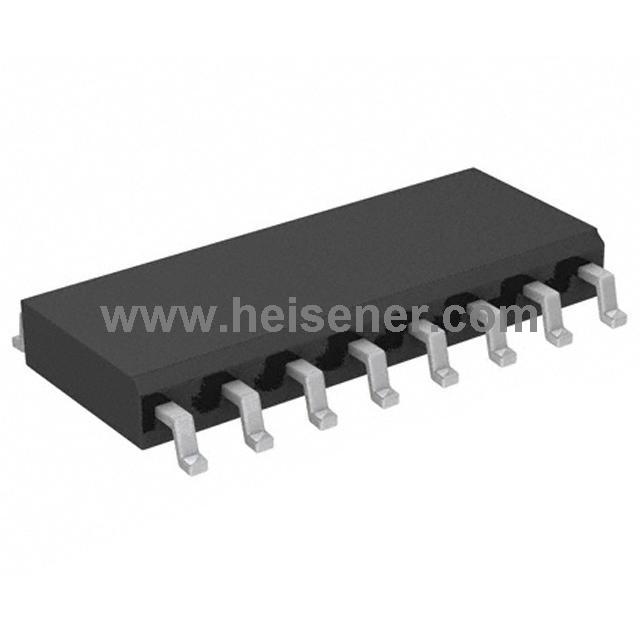
The EPCS4SI8N uses an 8-SOIC package, which is a very common type of surface-mount technology (SMT) package. It's known for its small form factor, with two rows of pins (four pins per side, for a total of eight). The pins extend outward from the sides of the package in a gull-wing shape, and the standard pin pitch is 1.27 mm. The body width is typically around 3.9 mm, providing a reliable solution for high-density layouts on PCBs.

EPCS4SI8N is a serial configuration memory (Serial PROM) used to store FPGA configuration data. It allows the FPGA to load its design upon power-up.
Connect VCC and GND properly. Use nCS to select the chip, DCLK for the clock, SDI to write data, and DO to read data. Make sure the timing is correct to avoid errors.
Ensure correct power supply voltage
Follow the proper timing for nCS, DCLK, SDI, and DO
Avoid static discharge as it can damage the chip