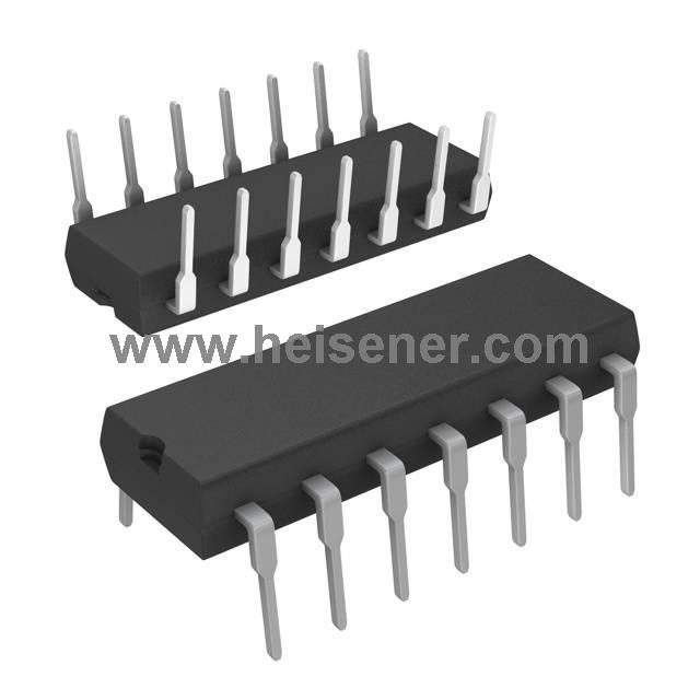
IR2110 Introduction
The IR2110 is a high-voltage, high-speed driver for controlling power MOSFETs and IGBTs, featuring independent high and low side output channels. It utilizes proprietary HVIC and latch-immune CMOS technologies, ensuring robust monolithic construction. The IR2110 is compatible with standard CMOS or LSTTL logic inputs, including 3.3V logic levels.
The driver’s output stage is optimized for high pulse current, minimizing cross-conduction. Matched propagation delays make it ideal for high-frequency applications, and its floating channel can drive an N-channel power MOSFET or IGBT in high-side configurations, supporting voltages up to 500 or 600 volts.
IR2110 Pinout

LO: Low-side gate drive output, connects to the gate of the low-side MOSFET.
COM: Common ground reference for the low-side driver.
VCC: Low-side and logic fixed supply voltage, typically 10V to 20V.
VS: High-side floating supply return, connects to the source of the high-side MOSFET.
VB: High-side floating supply voltage, provides power to the high-side driver.
HO: High-side gate drive output, connects to the gate of the high-side MOSFET.
VDD: Logic power supply, typically 3.3V or 5V.
HIN: Logic input for high-side gate driver, active high.
SD: Shutdown input, active low, disables both high and low-side outputs when active.
LIN: Logic input for low-side gate driver, active high.
VSS: Logic ground.
IR2110 Symbol

IR2110 Footprint

IR2110 3D Model

IR2110 Typical Connection

IR2110 Functional Block Diagram

IR2110 Specification
| Specification | Value |
| Supply Voltage (Vcc) | 10V to 20V |
| High-Side Floating Supply Voltage (V_B) | Up to 500V/600V |
| Output Source Current | 2A |
| Output Sink Current | 2A |
| Voltage - Supply | 3.3V ~ 20V |
| Propagation Delay | 120ns |
| Logic Voltage - VIL, VIH | 6V, 9.5V |
| Number of Drivers | 2 |
| Turn-On Time | 120ns |
| Turn-Off Time | 94ns |
| Operating Temperature Range | -40°C - 150°C |
| Package Type | 14-DIP |
IR2110 Features
Floating channel designed for bootstrap operation Fully operational to +500V or +600V Tolerant to negative transient voltage dV/dt immune
Gate drive supply ranges from 10 to 20V
Undervoltage lockout for both channels
3.3V logic compatible Separate logic supply range from 3.3V to 20V Logic and power ground ±5V offset
CMOS Schmitt-triggered inputs with pull-down
Cycle by cycle edge-triggered shutdown logic
Matched propagation delay for both channels
Outputs in phase with inputs
IR2110 Applications
Switch-Mode Power Supplies (SMPS)
DC-DC Converters
Motor Control
Uninterruptible Power Supplies (UPS)
Induction Heating
Lighting Ballasts
Resonant Converters
Renewable Energy Systems
How to Use IR2110?
1. Connect the logic power supply to VDD and the low voltage supply to VCC, then ground the COM and VSS pins.
2. Connect the high-side and low-side MOSFETs to the HO and LO pins, respectively. Connect the source of the high-side MOSFET to the VS pin, and the VB pin to the high-voltage power supply to drive the high-side MOSFET.
3. Control the high-side and low-side MOSFETs by inputting control signals to the HIN and LIN pins, which will turn them on and off, respectively.
4. To shut down all outputs, pull the SD pin low to enter shutdown mode.
IR2110 Package

FAQs
What is the IR2110 used for?
The IR2110 is a high-voltage, high-speed MOSFET and IGBT driver, used to control both high-side and low-side power transistors in applications like motor control, power supplies, and inverters.
How do I connect the IR2110?
The IR2110 requires connections for logic power (VDD), low-voltage power (VCC), ground (COM and VSS), and the gate of the MOSFETs (HO for high-side, LO for low-side). The source of the high-side MOSFET should connect to VS, and VB should connect to the high-voltage power supply.
What logic levels are compatible with the IR2110?
The IR2110 is compatible with standard CMOS or LSTTL logic levels, including 3.3V and 5V logic.