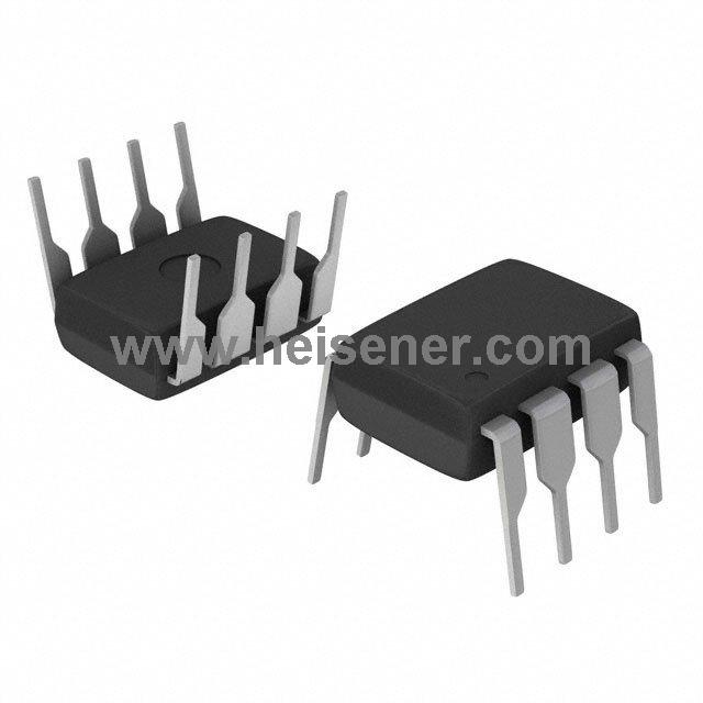
IR2184 Introduction
The IR2184 is a high-voltage, high-speed driver designed for power MOSFETs and IGBTs, featuring dependent high and low side referenced output channels. Utilizing proprietary HVIC and latch-immune CMOS technologies, it ensures robust monolithic construction.
It supports standard CMOS or LSTTL logic inputs down to 3.3V and includes high pulse current buffer stages to minimize cross-conduction. Its fl oating channel allows driving N-channel power MOSFETs or IGBTs in high-side configurations, operating up to 600 volts, making it ideal for demanding power electronics applications.
IR2184 Pinout
IN: Logic input for high and low side gate driver outputs (HO and LO), in phase with HO (referenced to COM for IR2184)
SD: Logic input for shutdown (referenced to COM for IR2184)
COM: Low side return
LO: Low side gate drive output
VCC: Low side and logic fixed supply
VS: High side floating supply return
HO: High side gate drive output
VB: High side floating supply
IR2184 Typical Connection

IR2184 Functional Block Diagram

IR2184 Specification
| Parameter | Specification |
| Driver Type | Half-Bridge |
| Input Logic Compatibility | CMOS or LSTTL (down to 3.3V logic) |
| Supply Voltage | 10V ~ 20V |
| Logic Voltage - VIL, VIH | 0.8V, 2.7V |
| Max High Side Voltage | 600 V |
| Peak Output Current | 1.9A, 2.3A |
| Rise / Fall Time | 40ns, 20ns |
| Cross-Conduction Protection | Yes |
| Technology | HVIC and latch-immune CMOS |
| Package Options | 8-PDIP |
| Operating Temperature | -40°C ~ 150°C |
IR2184 Features
Floating channel designed for bootstrap operation
Fully operational to +600V
Tolerant to negative transient voltage
dV/dt immune
Gate drive supply ranges from 10 to 20V
Undervoltage lockout for both channels
3.3V and 5V input logic compatible
Matched propagation delay for both channels
Logic and power ground +/- 5V offset.
Lower di/dt gate driver for better noise immunity
Output source/sink current capability 1.4A/1.8A
Also available LEAD-FREE (PbF)
IR2184 Applications
AC/DC Motor Control Systems
Uninterruptible Power Supplies (UPS)
Industrial Inverters
Solar Inverters
Switch-Mode Power Supplies (SMPS)
HVAC Systems
Appliance Control
Battery-Powered Systems
IR2184 Package
The 8-PDIP package of the IR2184 is a standard through-hole design, featuring a compact and user-friendly structure that suits various PCB layout requirements. Its package dimensions include a maximum length of 9.81 mm, a width of 7.11 mm, and a height of 3.94 mm, with a pin pitch of 2.54 mm and a typical pin thickness of 0.356 mm. This package type offers excellent mechanical strength and is well-suited for both manual soldering and automated assembly processes.

How to Test and Connect IR2184?
To test and connect the IR2184, follow these steps to ensure proper functionality and safe integration into the circuit.
Prepare a test circuit for the IR2184 with a DC power supply, signal generator, load resistors, and high-voltage protection. Connect VCC to a low-voltage supply and COM to ground. Attach the signal generator output to IN for switching control, and ground SD or connect it to VCC via a resistor to enable the chip. Connect VS and VB to a high-voltage supply for the high-side floating circuit, linking VS to the test load's high-side reference.
Gradually power up and monitor LO and HO outputs to ensure proper logic-driven signals. Test voltage and waveforms under no-load conditions to confirm signal stability. After validation, connect the IR2184 to a load (e.g., MOSFETs or IGBTs), ensuring correct high- and low-side driving. Adjust input frequency and duty cycle to evaluate response and performance.
IR2181/IR2183/IR2184 Comparison

FAQs
What is IR2184 used for?
The IR2184 is a high-voltage, high-speed gate driver designed for driving both high-side and low-side power MOSFETs or IGBTs in half-bridge configurations, commonly used in motor drives, inverters, and power supply circuits.
How is the IR2184 protected from cross-conduction?
The IR2184 includes a high-pulse-current buffer stage and internal logic design to minimize driver cross-conduction, ensuring stable and efficient operation.
How is the IR2184 tested and connected in a circuit?
A test circuit typically includes a DC power supply, signal generator, and load resistors. VCC is connected to a low-voltage supply, COM is grounded, and VS and VB are connected to a high-voltage supply. The IN pin controls the high- and low-side outputs, and the SD pin enables or disables the driver.