The AT24C32A/64A provides 32,768/65,536 bit serial electrically erasable and programmable read-only memory (EEPROM), organized into 4096/8192 8-bit words. The cascading nature of the device allows up to eight devices to share a common 2-wire bus. The equipment is optimized for many industrial and commercial applications where low power and low voltage operations are essential.
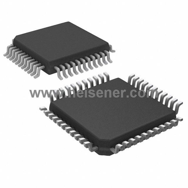
Pin Configurations

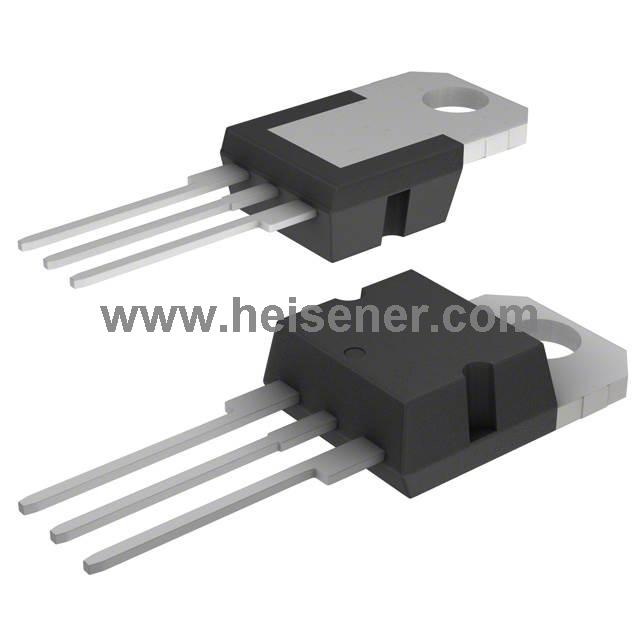
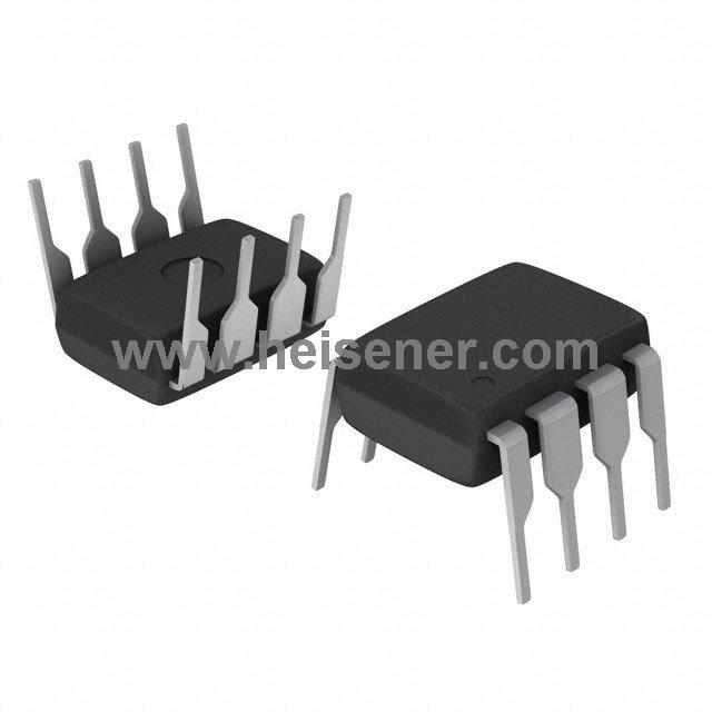
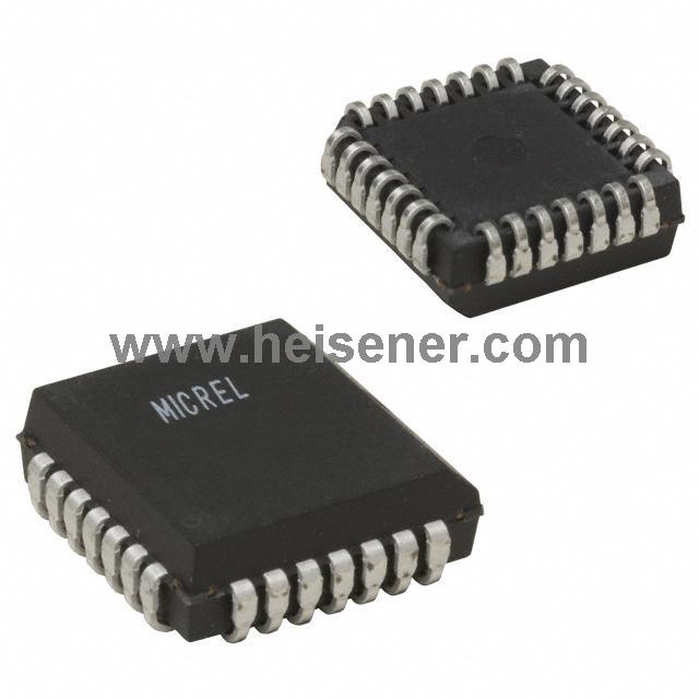
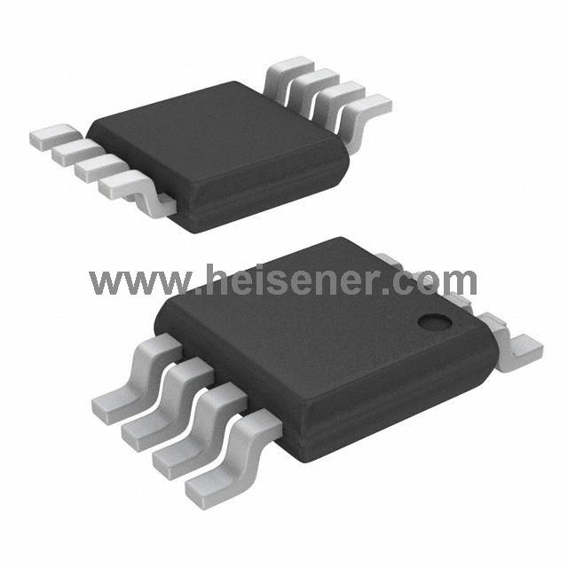
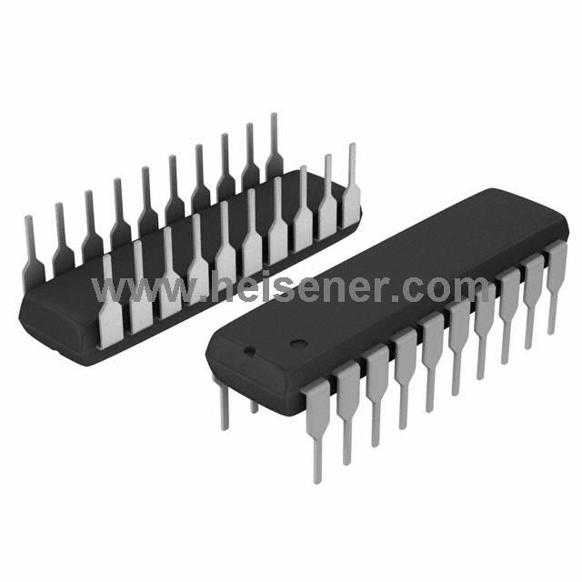
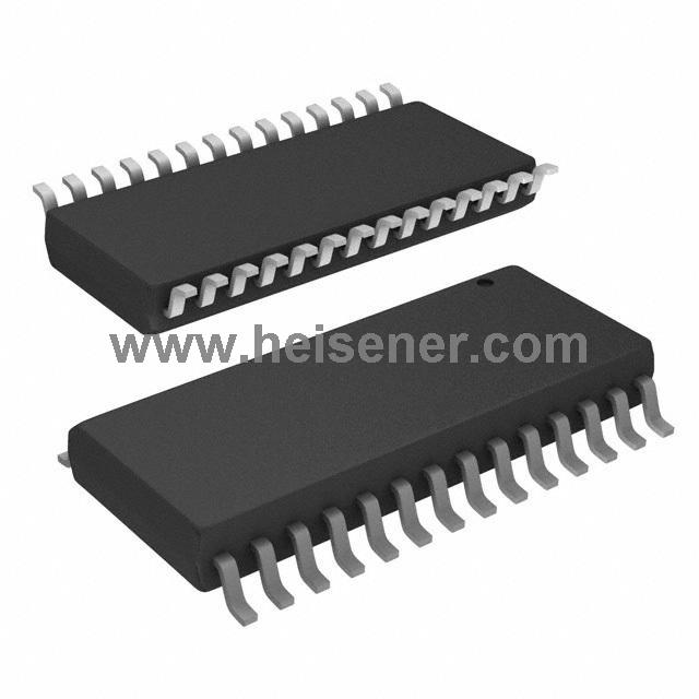
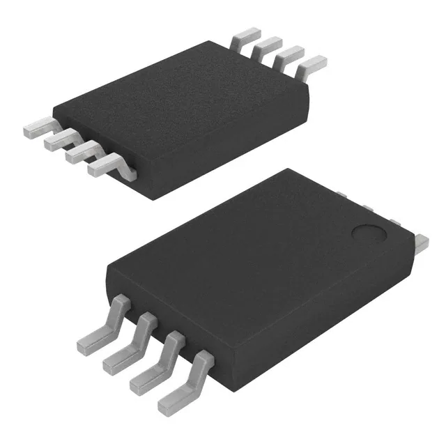
The AT24C32A/64A is offered in space-saving 8-lead JEDEC PDIP, 8-lead JEDEC SOIC, 8-lead EIAJ SOIC, 8-lead MAP and 8-lead TSSOP packages and is accessed via a 2-wire serial interface. In addition, the entire series is available in 2.7V (2.7V to 5.5V) and 1.8V (1.8V to 5.5V) versions.
Block Diagram

Pin Description
(1)Serial Clock (SCL): The SCL input is used to input positive edge clock data to each EEPROM device and output negative edge clock data to each device.
(2)SERIAL DATA (SDA): The SDA pin is used for bidirectional serial data transmission. The pin is leak-driven and can be routed with any number of other leak-opening or open-collector devices.
(3)DEVICE/ADDRESSES (A2, A1, A0): Pins A2, A1, and A0 are device address inputs and are hardwired or unconnected for hardware compatibility with other AT24Cxx devices. When the pins are hardwired, there may be up to eight 32K/64K device addresses on a single bus system (device addressing is discussed in detail in the Device addressing section). If the pin is floating, if the capacitor is coupled to the board the VCC plane is < 3 pF, then pins A2, A1, and A0 will be internally pulled to GND. If the coupling is > 3 pF, Atmel recommends that the address pins be connected to GND.
(4)WRITE PROTECT (WP): Allows normal write operations when the input is connected to GND. When WP is highly connected to VCC, all writes to memory are suppressed. If the pin is floating, if the capacitor is coupled to the board the VCC plane is < 3 pF, then the WP pin will be internally pulled to GND. If the coupling is > 3 pF, Atmel recommends connecting the pins to GND. Switching WP to VCC before a write operation creates software write protection.