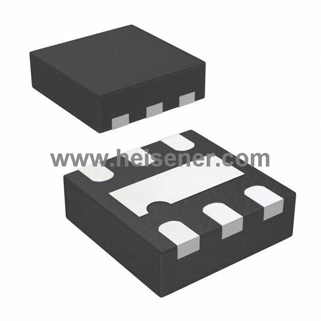
The SST25WF080 is a member of the Serial Flash 25 family and features a four-wire, SPI-compatible interface that allows low-pin number packaging, takes up less board space and ultimately reduces the total system cost. Available in 8-pin, 150mil SOIC package and 8-bump XFBGA package.
Pin Description
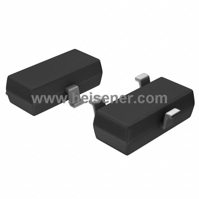
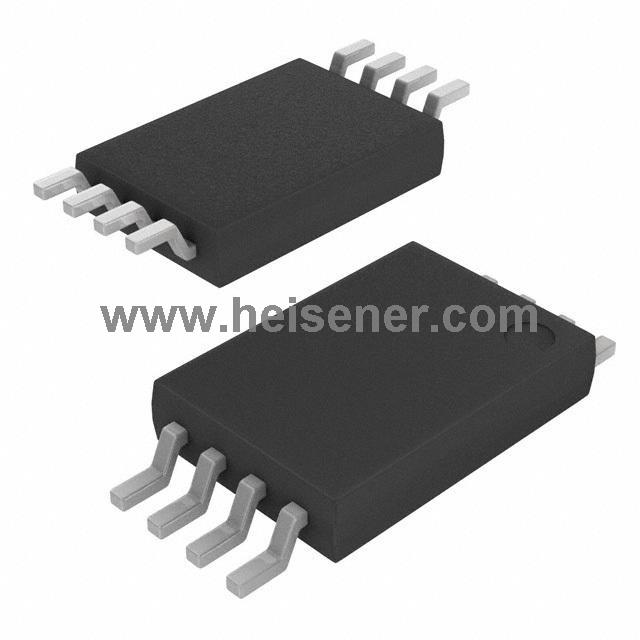
Pin Assignment for 8-Lead SOIC

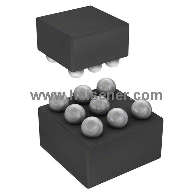
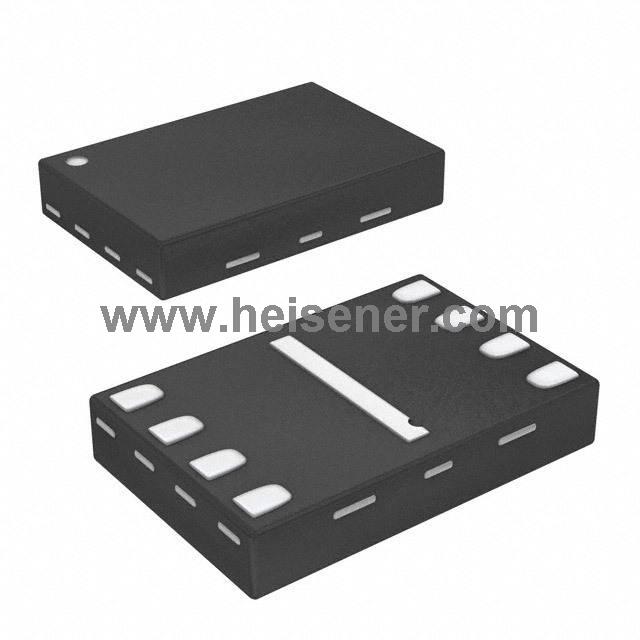
Pin Assignment for 8-bump XFBGA

The SST25WF080 SPI serial Flash memory is manufactured using SST's proprietary high performance CMOS SuperFlash technology. The separation gate chamber design and thick oxide tunnel injector provide better reliability and manufacturability than other methods.
The SST25WF080 significantly improves performance and reliability while reducing power consumption. The device is written (programmed or erased) with SST25WF080 single power supply of 1.65-1.95V. The total energy consumed is a function of applied voltage, current, and applied time. Since SuperFlash technology uses less current to program over any given voltage range and has a shorter erase time, the total energy consumed in any erase or program operation is less than other flash technologies.
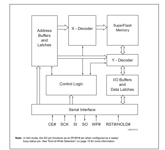
Functional Block Diagram
Device Operation
SST25WF080 is accessed via SPI(Serial Peripheral Interface) bus compatible protocol. SPI bus consists of four control lines; ce# (Chip Enable) is used to select devices and access data through three methods: SI (Serial data Input), SO (Serial data Output), and SCK (Serial Clock).
SST25WF080 supports SPI bus operations for both mode 0(0,0) and mode 3(1,1). As shown in the figure below, the difference between the two modes is that the bus host is in standby mode and there is no SCK signal for data transfer. The SCK signal was low in mode 0 and high in mode 3. For both modes, the serial data input (SI) is sampled at the rising edge of the SCK clock signal, and the serial data output (SO) is driven at the falling edge of the SCK clock signal.
SPI protocol

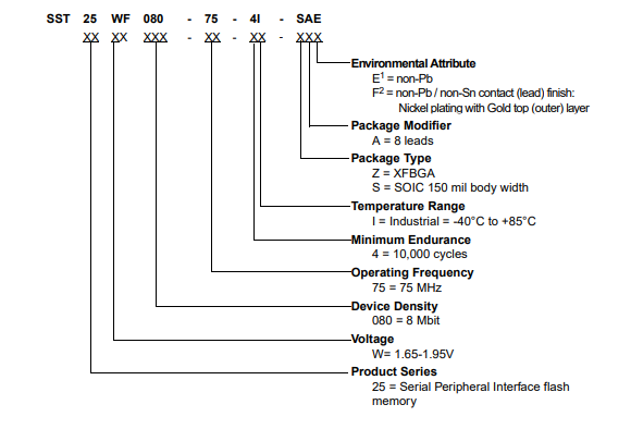
Product Ordering Information
Features
● Single voltage read/write operation
- 1.95-1.65v
● Serial interface architecture
- SPI Compatible: Mode 0 and Mode 3
● High speed clock frequency
- 75 MHz
● High reliability
- Endurance :100,000 cycles (typical)
- Over 100 years of data retention
● Ultra-low power consumption:
- Active reading current :2 mA(typical @33 MHz)
- Standby current :5µA(typical)
● Flexible erasure capability
- Uniform 4kbyte sectors
- Unified 32kbyte coverage block
- Uniform 64kbyte coverage blocks
● Quick erase and byte programs:
- Chip erase time: 35ms (typical)
- Sector -/ block - Erase time: 18ms (typical)
- Byte program time :14µS(typical)
● Automatic address increment (AAI) programming
- Reduces the total chip programming time for byte program operations
● Write end detection
- The BUSY bit in the software polling status register
- Busy state read SO pin
● Reset pin (RST#) or programmable hold pin The (#) option
- The default hardware reset pin is used
- Hold the pin option to pause a serial sequence without Deselect device
● Write protection (WP#)
- Enables or disables the status lock function register
● Software write protection
- Write protection is implemented using block protection bits in the state register
● Temperature range
- Industrial :-40℃~ +85℃
● Available Software packages
- 8 Lead SOIC(150 mil)
- 8-bump XFBGA
● All equipment is RoHS compliant