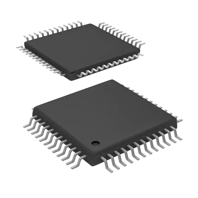
The DAC5652 is a single-chip, dual-channel, 10-bit high-speed DAC with on-chip reference voltage. 48 pin TQFP package. Pin compatibility between family members provides 10-bit (DAC5652), 12-bit (DAC5662), and 14-bit (DAC5672) resolutions. In addition, the DAC5652 is compatible with the DAC2900 and AD9763 dual Dacs. The equipment is characterized to operate in the industrial temperature range of -40°C to 85°C.
DAC5652 Pin information

With update rates up to 275 MSPS, the DAC5652 provides excellent dynamic performance, tight gain and offset matching features, making it suitable for I/Q baseband or direct IF communication applications. Each DAC has a high impedance, differential current output and is suitable for single ended or differential analog output configurations.
External resistors allow the full-scale output current to be scaled for each DAC individually or together, typically between 2 mA and 20 mA. The precise on-chip voltage reference is temperature compensated and provides a stable 1.2v reference voltage. Optionally, use external references. The DAC5652 has two 10-bit parallel input ports with separate clocks and data latches.
For flexibility, the DAC5652 also supports multiplex data for each DAC at one port while operating in interlaced mode, and is designed specifically for differential transformer coupling outputs with 50-Ω double-terminal loads. For 20ma full-scale output current, both 4:1 impedance ratio (output power of 4dbm) and 1:1 impedance ratio transformer (output power of -2 dBm) are supported.
DAC5652 Functional block diagram

Digital input and timing
Digital Inputs
The DAC5652 data entry port accepts a standard positive encoding, where the data bits DA9 and DB9 are the most significant bits (MSB). The converter output supports clock rates up to 275 MSPS. The best performance is usually achieved by achieving a symmetrical write and clock duty cycle; However, duty cycle can vary as timing specifications are met. Similarly, set and hold times can be selected within their specified limits.
All digital inputs in DAC5652 are CMOS compatible. The following two diagrams show the schematic diagram of the DAC5652 equivalent CMOS digital input. Pull-up and pull-down circuits are approximately equivalent to 100kω. The 10-bit data input follows the offset positive binary encoding scheme. DAC5652 Designed for 3v to 3.6V Digital Power Supply (DVDD)
CMOS/TTL digital equivalent input with internal pull-down resistor

CMOS/TTL digital equivalent input with internal pull-up resistor

Input interface
The DAC5652 has two working modes selected by the MODE pin, as shown below.
(1) For dual-bus input mode, the device basically consists of two independent Dacs. Each DAC has its own separate data input bus, clock input, and data write signals (data latches).
(2) In single-bus interleaving mode, data must be interleaved on the A-channel input bus. This mode does not use the B-channel input bus. The clock and write input are now shared by the two Dacs.
Double bus mode operation
