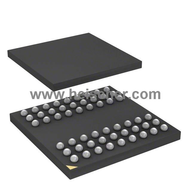
The W25Q128JVSIQ is a 128M-bit serial Flash memory device. It operates on a 2.7V to 3.6V power supply and supports low-power operation. In power-down mode, current consumption can drop to the microamp level, making it suitable for power-sensitive applications. The device supports standard SPI as well as Dual and Quad SPI interfaces. It can be used for code storage, data storage, and execute-in-place (XIP) applications. It is widely used in industrial control, consumer electronics, and smart devices.
In terms of memory organization, the W25Q128JVSIQ contains 65,536 programmable pages of 256 bytes each and supports page-based programming. It also offers flexible erase options, including 4KB sector erase, 32KB and 64KB block erase, and full chip erase. This allows efficient data management based on system needs. With a high-speed SPI clock of up to 133MHz, the device achieves higher data transfer rates in Dual and Quad modes, delivering performance comparable to or even better than some parallel Flash memories.

/CS: Chip Select Input
DO (IO1): Data Output (Data Input Output 1)(1)
/WP (IO2): Write Protect Input ( Data Input Output 2)(2)
GND: Ground
DI (IO0): Data Input (Data Input Output 0)(1)
CLK: Serial Clock Input
/HOLD or /RESET (IO3): Hold or Reset Input (Data Input Output 3)(2)
VCC: Power Supply


| Parameter | Specification |
| Part Number | W25Q128JVSIQ |
| Memory Type | Non-Volatile |
| Manufacturer | Winbond Electronics |
| Density | 128 Mbit (16 MB) |
| Memory Organization | 16M x 8 |
| Memory Interface | SPI - Quad I/O, QPI |
| Operating Voltage | 2.7 V – 3.6 V |
| Max SPI Clock Frequency | 133 MHz |
| Execute-In-Place (XIP) | Supported |
| Page Size | 256 bytes |
| Pages | 65,536 |
| Sector Size | 4 KB |
| Number of Sectors | 4,096 |
| Block Sizes | 32 KB, 64 KB |
| Number of Blocks | 256 (64 KB blocks) |
| Program Operation | Page Program |
| Write Cycle Time - Word, Page | 3ms |
| Low-Power Mode | Power-Down Mode |
| Power-Down Current | ~1 µA (typical) |
| Data Retention | 20 years (typical) |
| Endurance | 100,000 Program/Erase cycles |
| Package | 8-SOIC |
| Operating Temperature | -40°C ~ 85°C (TA) |
| Base Product Number | W25Q128 |
New Family of SpiFlash Memories
– W25Q128JV: 128M-bit / 16M-byte
– Standard SPI: CLK, /CS, DI, DO
– Dual SPI: CLK, /CS, IO0, IO1
– Quad SPI: CLK, /CS, IO0, IO1, IO2, IO3
– Software & Hardware Reset(1)
Highest Performance Serial Flash
– 133MHz Single, Dual/Quad SPI clocks
– 266/532MHz equivalent Dual/Quad SPI
– 66MB/S continuous data transfer rate
– Min. 100K Program-Erase cycles per sector
– More than 20-year data retention
Efficient "Continuous Read"
– Continuous Read with 8/16/32/64-Byte Wrap
– As few as 8 clocks to address memory
– Allows true XIP (execute in place) operation
Low Power, Wide Temperature Range
– Single 2.7 to 3.6V supply
– <1µA Power-down (typ.)
– -40°C to +85°C operating range
– -40°C to +105°C operating range
Flexible Architecture with 4KB sectors
– Uniform Sector/Block Erase (4K/32K/64K-Byte)
– Program 1 to 256 byte per programmable page
– Erase/Program Suspend & Resume
Advanced Security Features
– Software and Hardware Write-Protect
– Power Supply Lock-Down – Special OTP protection
– Top/Bottom, Complement array protection
– Individual Block/Sector array protection
– 64-Bit Unique ID for each device
– Discoverable Parameters (SFDP) Register
– 3X256-Bytes Security Registers with OTP locks
– Volatile & Non-volatile Status Register Bits
Space Efficient Packaging
– 8-pin SOIC 208-mil
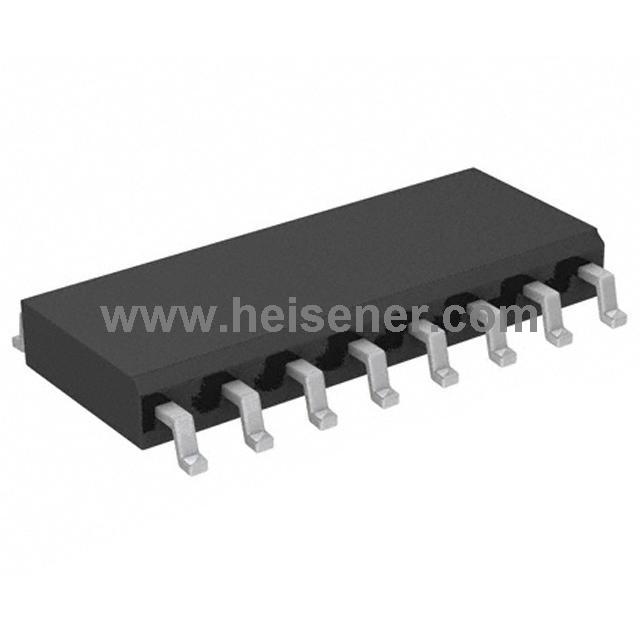
– 16-pin SOIC 300-mil (additional /RESET pin)
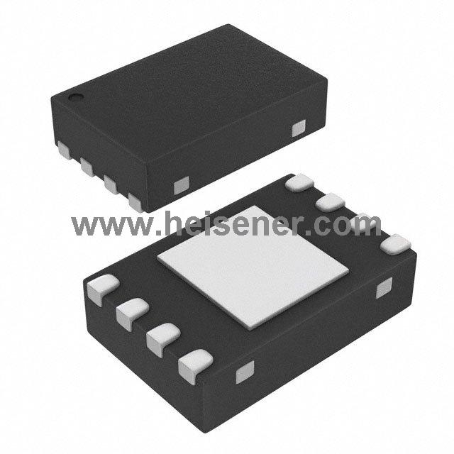
– 8-pad WSON 6x5-mm / 8x6-mm
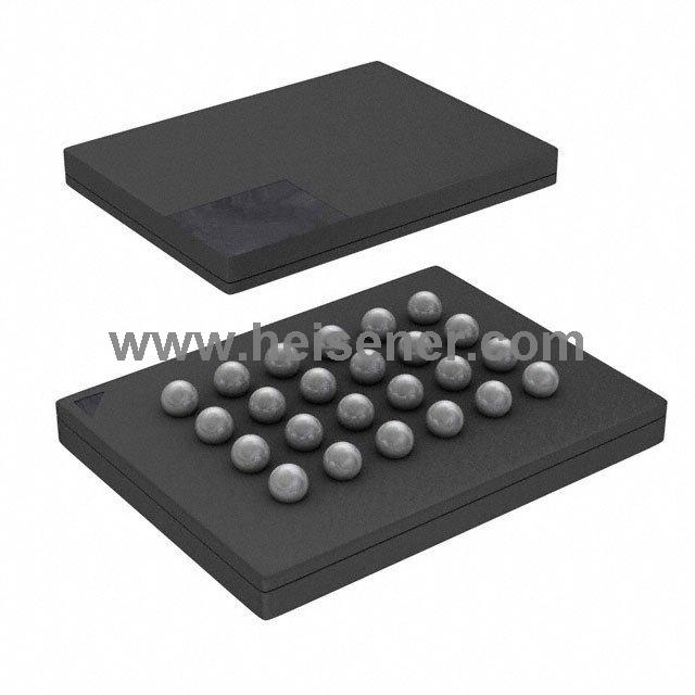
– 24-ball TFBGA 8x6-mm (6x4/5x5 ball array)
– 24-ball WLCSP
– Contact Winbond for KGD and other options
Industrial Control Systems
Embedded Systems
Consumer Electronics
IoT Devices
Execute-In-Place (XIP) Applications
Data Logging and Storage
Medical and Measurement Equipment
Automotive and Smart Modules (Non-safety)

From the W25Q128JV Serial Flash Memory block diagram, the device consists of a memory array, address and control logic, an SPI interface, and internal high-voltage and buffer blocks. The memory array uses a layered structure, with 256-byte pages as the smallest program unit, organized into 4KB sectors and 64KB blocks for flexible erase and management. Blocks 0 to 255 are clearly defined, and the device supports 4KB, 32KB, 64KB, and full-chip erase. The SFDP register and Security Registers 1–3 are used for device identification and secure data storage.
In the control and interface section, the W25Q128JV communicates with the MCU through SPI command and control logic and supports standard SPI as well as Dual and Quad I/O modes. Address latches manage page and byte addresses for accurate access, while column decoding and a 256-byte page buffer improve read and write efficiency. Write control logic, status registers, and internal high-voltage generators support reliable program and erase operations, making the device suitable for embedded systems and XIP applications.
1. Standard SPI
The W25Q128JV communicates via a standard SPI interface (CLK, /CS, DI, DO). Data is written on the rising edge of CLK and read on the falling edge. It supports SPI Mode 0 and Mode 3, which differ in the default CLK level when idle.
2. Dual SPI
Dual SPI read commands are supported, such as Fast Read Dual Output and Dual I/O. Data transfer speed is faster than standard SPI. The DI and DO pins serve as bidirectional IO0 and IO1, making it suitable for code loading and XIP (Execute In Place) applications.
3. Quad SPI
Quad SPI read commands are supported, such as Fast Read Quad Output and Quad I/O. This allows even higher transfer speeds. The four bidirectional data pins are used (IO0, IO1, IO2, and IO3).
4. Reset Function
Both software and hardware resets are supported. Software reset is executed via the 66h and 99h commands, with a reset time of approximately 30 µs. Some packages include a hardware /RESET pin, which has higher priority than SPI signals.
5. Write Protection
The device includes multiple built-in write protection mechanisms to prevent data corruption caused by noise or abnormal conditions, enhancing data reliability.
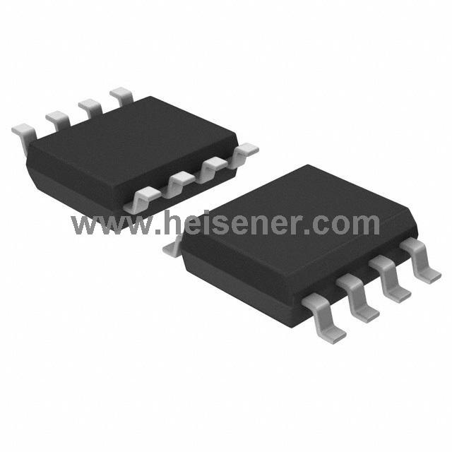
The W25Q128JVSIQ comes in an 8-SOIC package, which helps save space in various electronic devices. This package not only supports the standard SPI interface but is also compatible with Dual SPI and Quad SPI modes. The following are the detailed dimensions for this package:

It is a 128Mb serial NOR flash memory from Winbond, featuring high-speed SPI communication and compact 8-SOIC packaging.
It supports Standard SPI, Dual SPI, and Quad SPI modes for flexible and fast data transfer.
Yes, it supports both software reset (via 66h and 99h commands) and hardware reset through the /RESET pin.
It is ideal for code storage, firmware updates, and XIP (Execute In Place) applications in embedded systems, consumer electronics, and industrial devices.
W25Q128JVSIQ and other electronic parts are available from Heisener Electronics, a global distributor offering large in-stock inventory and fast delivery for OEMs, EMS providers, and electronics design companies.